


Samsung arrived at NVIDIA’s GTC 2026 conference in San Jose with a clear intent that it wants to be the company that supplies nearly every critical memory component inside tomorrow’s AI systems.
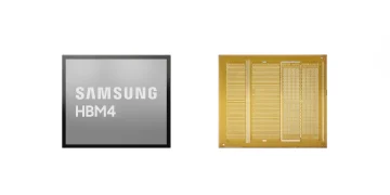
The headline product is HBM4, Samsung’s sixth-generation High Bandwidth Memory, which is now in mass production and built specifically for NVIDIA’s upcoming Vera Rubin platform.
HBM4 runs at 11.7 gigabits per second as standard, already beating the industry baseline of 8 Gbps, with the ability to push that to 13 Gbps.
Samsung achieved this using its most advanced 10-nanometer DRAM manufacturing process, called 1c, and says it has reached stable production yields at that node, which is the part that actually matters for shipping at scale.
READ: Samsung Retains No.1 Spot in Soundbars for 12th Year Running
Beyond HBM4, Samsung also pulled the curtain back on HBM4E for the first time, its next step up, capable of 16 Gbps per pin and 4.0 terabytes per second of total bandwidth.
That’s not in production yet, but it gives a clear picture of where high-end AI memory is heading.
One of the more technically interesting things on display is Samsung’s hybrid copper bonding (HCB) technology. Current HBM stacks are assembled using a method called thermal compression bonding.
HCB replaces that with copper-to-copper connections, which allows stacking 16 or more memory layers while cutting heat resistance by more than 20%.
More layers means more capacity, and less heat means the chip can sustain performance without throttling, both things AI accelerators desperately need.
Samsung also dedicated a section of its booth to products built around the NVIDIA partnership specifically. This includes SOCAMM2, a low-power server memory module designed for AI infrastructure that Samsung says is the first of its kind to reach mass production.
There are also two SSDs on show: the PM1763, built on the PCIe 6.0 interface for fast data transfers at high capacity, and the PM1753, which is part of NVIDIA’s BlueField-4 STX reference architecture and aimed at improving energy efficiency during AI inference workloads.
On the device side, Samsung is showing LPDDR5X and LPDDR6, the memory that goes inside smartphones, tablets, and wearables. LPDDR5X runs at up to 25 Gbps per pin while using 15% less power than its predecessor.
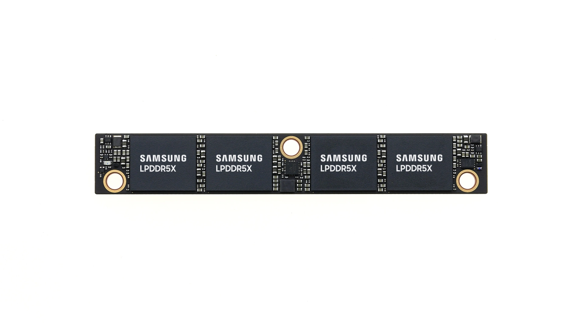
LPDDR6 goes further, hitting 30 to 35 Gbps per pin, and adds smarter power management features like adaptive voltage scaling and dynamic refresh control, which help edge AI applications run efficiently on battery-powered devices.
The two companies are also collaborating on Samsung’s internal manufacturing operations. Samsung plans to use NVIDIA’s accelerated computing tools and Omniverse platform to build digital twins of its own chip fabrication facilities.
Essentially, these are virtual replicas of real factories that can be used to simulate and optimize production. Samsung’s EVP of AI, Yong Ho Song, presented on this specifically on March 17, covering how agentic AI is being applied across chip design, engineering, and production.
READ: Samsung Has Been the World’s Top TV Brand for 20 Years Straight
What’s interesting about Samsung’s position here is the breadth. Most companies at an event like GTC are showing one piece of the puzzle.
Samsung is showing the memory that goes in the AI server, the storage that sits alongside it, the low-power memory that goes in your phone, and the manufacturing technology used to make all of it.
Whether that full-stack pitch translates into dominant market share is another question, but the technology on display is real, and most of it is already shipping.


